
----------------------------------------------------------------------------------
-- Company:
-- Engineer:
--
-- Create Date: 11:10:07 05/14/2011
-- Design Name:
-- Module Name: Lab3Q1 - Behavioral
-- Project Name:
-- Target Devices:
-- Tool versions:
-- Description:
--
-- Dependencies:
--
-- Revision:
-- Revision 0.01 - File Created
-- Additional Comments:
--
----------------------------------------------------------------------------------
library IEEE;
use IEEE.STD_LOGIC_ARITH.ALL;
use IEEE.STD_LOGIC_UNSIGNED.ALL;
use IEEE.STD_LOGIC_1164.ALL;
use IEEE.numeric_bit.all;
-- Uncomment the following library declaration if using
-- arithmetic functions with Signed or Unsigned values
--use IEEE.NUMERIC_STD.ALL;
-- Uncomment the following library declaration if instantiating
-- any Xilinx primitives in this code.
--library UNISIM;
--use UNISIM.VComponents.all;
entity RAMController is
Port ( RD : in STD_LOGIC;
WR : in STD_LOGIC;
reset : in STD_LOGIC;
Clk : in STD_LOGIC;
EN : in STD_LOGIC;
ADDRIN : in STD_LOGIC_VECTOR (15 downto 0);
ADDROUT : out STD_LOGIC_VECTOR ( 7 downto 0);
WE : out STD_LOGIC;
RAS : out STD_LOGIC;
CAS : out STD_LOGIC);
end RAMController;
architecture Behavioral of RAMController is
TYPE State_type IS (RASData, RASHigh, CASData,CASHigh,ReadData,WriteData, highImpedence);
SIGNAL state,nextState : State_type ;
begin
PROCESS (Reset, Clk, EN)
BEGIN
IF (Reset = '1') THEN
state <= RASData ;
ELSIF (EN = '1') THEN
IF (Clk'EVENT AND Clk = '1') THEN
state<=nextState;
END IF;
END IF;
END PROCESS;
PROCESS (state,ADDRIN,RD,WR)
BEGIN
CASE state IS
WHEN RASData =>
CAS <= '0';
WE <= '0';
RAS <= '0';
ADDROUT <= ADDRIN(15 downto 8);
nextState <= RASHigh;
WHEN RASHigh =>
ADDROUT <= ADDRIN(15 downto 8);
RAS <= '1';
CAS <= '0';
WE <= '0';
IF ((RD='1' and WR ='1')or(RD='0' and WR ='0')) then
nextState <= RASData;
ELSE
nextState <= CASData;
END IF;
WHEN CASData =>
RAS <= '0';
CAS <= '0';
WE <= '0';
ADDROUT <= ADDRIN(7 downto 0);
nextState <= CASHigh;
WHEN CASHigh =>
ADDROUT <= ADDRIN(7 downto 0);
CAS <= '1';
RAS <= '0';
WE <= '0';
IF(RD='1' and WR ='0') THEN
nextState <= ReadData;
ELSIF(RD='0' and WR ='1') THEN
nextState <= WriteData;
ELSE
nextState <= highImpedence;
END IF;
WHEN ReadData =>
RAS <= '0';
CAS <= '0';
WE <= '0';
ADDROUT <= ADDRIN(7 downto 0);
nextState <= RASData;
WHEN WriteData =>
RAS <= '0';
CAS <= '0';
WE <= '1';
ADDROUT <= ADDRIN(7 downto 0);
nextState <= RASData;
WHEN highImpedence =>
RAS <= '0';
CAS <= '0';
WE <= 'Z';
ADDROUT <= ADDRIN(7 downto 0);
nextState <= RASData;
END CASE;
end process;
end Behavioral;
Question 1 – HDL Synthesis
=========================================================================
* HDL Synthesis *
=========================================================================
Performing bidirectional port resolution...
Synthesizing Unit <RAMController>.
Related source file is "C:/Users/LAU HUI YON/Desktop/HET378/Lab2/Lab3Q1/Lab3Q1.vhd".
Found finite state machine <FSM_0> for signal <state>.
-----------------------------------------------------------------------
| States | 7 |
| Transitions | 13 |
| Inputs | 2 |
| Outputs | 7 |
| Clock | Clk (rising_edge) |
| Clock enable | EN (positive) |
| Reset | reset (positive) |
| Reset type | asynchronous |
| Reset State | rasdata |
| Power Up State | rasdata |
| Encoding | automatic |
| Implementation | LUT |
-----------------------------------------------------------------------
Found 1-bit tristate buffer for signal <WE>.
Summary:
inferred 1 Finite State Machine(s).
inferred 1 Tristate(s).
Unit <RAMController> synthesized.
=========================================================================
HDL Synthesis Report
Macro Statistics
# Tristates : 1
1-bit tristate buffer : 1
=========================================================================
=========================================================================
* Advanced HDL Synthesis *
=========================================================================
Analyzing FSM <FSM_0> for best encoding.
Optimizing FSM <state/FSM> on signal <state[1:7]> with one-hot encoding.
---------------------------
State | Encoding
---------------------------
rasdata | 0000001
rashigh | 0000010
casdata | 0000100
cashigh | 0001000
readdata | 0010000
writedata | 0100000
highimpedence | 1000000
---------------------------
=========================================================================
Advanced HDL Synthesis Report
Macro Statistics
# FSMs : 1
=========================================================================
=========================================================================
* Low Level Synthesis *
=========================================================================
Optimizing unit <RAMController> ...
Mapping all equations...
Building and optimizing final netlist ...
Found area constraint ratio of 100 (+ 5) on block RAMController, actual ratio is 1.
Final Macro Processing ...
=========================================================================
Final Register Report
Macro Statistics
# Registers : 7
Flip-Flops : 7
Question 1 –TIMING REPORT
=========================================================================
TIMING REPORT
NOTE: THESE TIMING NUMBERS ARE ONLY A SYNTHESIS ESTIMATE.
FOR ACCURATE TIMING INFORMATION PLEASE REFER TO THE TRACE REPORT
GENERATED AFTER PLACE-and-ROUTE.
Clock Information:
------------------
-----------------------------------+------------------------+-------+
Clock Signal | Clock buffer(FF name) | Load |
-----------------------------------+------------------------+-------+
Clk | BUFGP | 7 |
-----------------------------------+------------------------+-------+
Asynchronous Control Signals Information:
----------------------------------------
-----------------------------------+------------------------+-------+
Control Signal | Buffer(FF name) | Load |
-----------------------------------+------------------------+-------+
reset | IBUF | 7 |
-----------------------------------+------------------------+-------+
Timing Summary:
---------------
Speed Grade: -5
Minimum period: 2.708ns (Maximum Frequency: 369.324MHz)
Minimum input arrival time before clock: 3.391ns
Maximum output required time after clock: 6.905ns
Maximum combinational path delay: 5.753ns
Timing Detail:
--------------
All values displayed in nanoseconds (ns)
=========================================================================
Timing constraint: Default period analysis for Clock 'Clk'
Clock period: 2.708ns (frequency: 369.324MHz)
Total number of paths / destination ports: 10 / 7
-------------------------------------------------------------------------
Delay: 2.708ns (Levels of Logic = 2)
Source: state_FSM_FFd6 (FF)
Destination: state_FSM_FFd7 (FF)
Source Clock: Clk rising
Destination Clock: Clk rising
Data Path: state_FSM_FFd6 to state_FSM_FFd7
Gate Net
Cell:in->out fanout Delay Delay Logical Name (Net Name)
---------------------------------------- ------------
FDCE:C->Q 6 0.514 0.599 state_FSM_FFd6 (state_FSM_FFd6)
LUT3_L:I2->LO 1 0.612 0.103 state_FSM_FFd7-In_SW0 (N7)
LUT4:I3->O 1 0.612 0.000 state_FSM_FFd7-In (state_FSM_FFd7-In)
FDPE:D 0.268 state_FSM_FFd7
----------------------------------------
Total 2.708ns (2.006ns logic, 0.702ns route)
(74.1% logic, 25.9% route)
=========================================================================
Timing constraint: Default OFFSET IN BEFORE for Clock 'Clk'
Total number of paths / destination ports: 17 / 12
-------------------------------------------------------------------------
Offset: 3.391ns (Levels of Logic = 3)
Source: RD (PAD)
Destination: state_FSM_FFd7 (FF)
Destination Clock: Clk rising
Data Path: RD to state_FSM_FFd7
Gate Net
Cell:in->out fanout Delay Delay Logical Name (Net Name)
---------------------------------------- ------------
IBUF:I->O 5 1.106 0.690 RD_IBUF (RD_IBUF)
LUT3_L:I0->LO 1 0.612 0.103 state_FSM_FFd7-In_SW0 (N7)
LUT4:I3->O 1 0.612 0.000 state_FSM_FFd7-In (state_FSM_FFd7-In)
FDPE:D 0.268 state_FSM_FFd7
----------------------------------------
Total 3.391ns (2.598ns logic, 0.793ns route)
(76.6% logic, 23.4% route)
=========================================================================
Timing constraint: Default OFFSET OUT AFTER for Clock 'Clk'
Total number of paths / destination ports: 71 / 11
-------------------------------------------------------------------------
Offset: 6.905ns (Levels of Logic = 4)
Source: state_FSM_FFd2 (FF)
Destination: ADDROUT<7> (PAD)
Source Clock: Clk rising
Data Path: state_FSM_FFd2 to ADDROUT<7>
Gate Net
Cell:in->out fanout Delay Delay Logical Name (Net Name)
---------------------------------------- ------------
FDCE:C->Q 4 0.514 0.651 state_FSM_FFd2 (state_FSM_FFd2)
LUT4:I0->O 1 0.612 0.000 ADDROUT<0>11 (ADDROUT<0>1)
MUXF5:I0->O 8 0.278 0.712 ADDROUT<0>1_f5 (N01)
LUT4:I1->O 1 0.612 0.357 ADDROUT<7>1 (ADDROUT_7_OBUF)
OBUF:I->O 3.169 ADDROUT_7_OBUF (ADDROUT<7>)
----------------------------------------
Total 6.905ns (5.185ns logic, 1.720ns route)
(75.1% logic, 24.9% route)
=========================================================================
Timing constraint: Default path analysis
Total number of paths / destination ports: 16 / 8
-------------------------------------------------------------------------
Delay: 5.753ns (Levels of Logic = 3)
Source: ADDRIN<7> (PAD)
Destination: ADDROUT<7> (PAD)
Data Path: ADDRIN<7> to ADDROUT<7>
Gate Net
Cell:in->out fanout Delay Delay Logical Name (Net Name)
---------------------------------------- ------------
IBUF:I->O 1 1.106 0.509 ADDRIN_7_IBUF (ADDRIN_7_IBUF)
LUT4:I0->O 1 0.612 0.357 ADDROUT<7>1 (ADDROUT_7_OBUF)
OBUF:I->O 3.169 ADDROUT_7_OBUF (ADDROUT<7>)
----------------------------------------
Total 5.753ns (4.887ns logic, 0.866ns route)
(84.9% logic, 15.1% route)
=========================================================================
Total REAL time to Xst completion: 5.00 secs
Total CPU time to Xst completion: 5.25 secs
-->
Total memory usage is 190124 kilobytes
Number of errors : 0 ( 0 filtered)
Number of warnings : 0 ( 0 filtered)
Number of infos : 0 ( 0 filtered)

Figure 1 Question 1 Schematic diagram
--------------------------------------------------------------------------------
-- Company:
-- Engineer:
--
-- Create Date: 22:47:49 05/16/2011
-- Design Name:
-- Module Name: C:/Users/LAU HUI YON/Desktop/HET378/Lab2/Lab3Q1/Lab1Q1testbench.vhd
-- Project Name: Lab3Q1
-- Target Device:
-- Tool versions:
-- Description:
--
-- VHDL Test Bench Created by ISE for module: RAMController
--
-- Dependencies:
--
-- Revision:
-- Revision 0.01 - File Created
-- Additional Comments:
--
-- Notes:
-- This testbench has been automatically generated using types std_logic and
-- std_logic_vector for the ports of the unit under test. Xilinx recommends
-- that these types always be used for the top-level I/O of a design in order
-- to guarantee that the testbench will bind correctly to the post-implementation
-- simulation model.
--------------------------------------------------------------------------------
LIBRARY ieee;
USE ieee.std_logic_1164.ALL;
-- Uncomment the following library declaration if using
-- arithmetic functions with Signed or Unsigned values
--USE ieee.numeric_std.ALL;
ENTITY Lab1Q1testbench IS
END Lab1Q1testbench;
ARCHITECTURE behavior OF Lab1Q1testbench IS
-- Component Declaration for the Unit Under Test (UUT)
COMPONENT RAMController
PORT(
RD : IN std_logic;
WR : IN std_logic;
reset : IN std_logic;
Clk : IN std_logic;
EN : IN std_logic;
ADDRIN : IN std_logic_vector(15 downto 0);
ADDROUT : OUT std_logic_vector(7 downto 0);
WE : OUT std_logic;
RAS : OUT std_logic;
CAS : OUT std_logic
);
END COMPONENT;
--Inputs
signal RD : std_logic := '0';
signal WR : std_logic := '0';
signal reset : std_logic := '0';
signal Clk : std_logic := '0';
signal EN : std_logic := '0';
signal ADDRIN : std_logic_vector(15 downto 0) := (others => '0');
--Outputs
signal ADDROUT : std_logic_vector(7 downto 0);
signal WE : std_logic;
signal RAS : std_logic;
signal CAS : std_logic;
-- Clock period definitions
constant Clk_period : time := 10 ns;
BEGIN
-- Instantiate the Unit Under Test (UUT)
uut: RAMController PORT MAP (
RD => RD,
WR => WR,
reset => reset,
Clk => Clk,
EN => EN,
ADDRIN => ADDRIN,
ADDROUT => ADDROUT,
WE => WE,
RAS => RAS,
CAS => CAS
);
-- Clock process definitions
Clk_process :process
begin
Clk <= '0';
wait for Clk_period/2;
Clk <= '1';
wait for Clk_period/2;
end process;
-- Stimulus process
stim_proc: process
begin
-- hold reset state for 100 ns.
wait for 100 ns;
wait for Clk_period*10;
-- insert stimulus here
ADDRIN <= "1000110011010110";
EN <= '1';
RAS <= '1';wait for 10 ns;
CAS <= '1';wait for 10 ns;
RD <= '0';
WR <= '1';wait for 10 ns;
RD <= '1';
WR <= '0';wait for 10 ns;
RD <= '1';
WR <= '1';wait for 10 ns;
wait;
end process;
END;

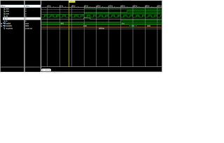
Figure 2 Question 1 testbench Simulation results
----------------------------------------------------------------------------------
-- Company:
-- Engineer:
--
-- Create Date: 23:19:42 05/17/2011
-- Design Name:
-- Module Name: Lab3Q2 - Behavioral
-- Project Name:
-- Target Devices:
-- Tool versions:
-- Description:
--
-- Dependencies:
--
-- Revision:
-- Revision 0.01 - File Created
-- Additional Comments:
--
----------------------------------------------------------------------------------
library IEEE;
use IEEE.STD_LOGIC_1164.ALL;
use IEEE.std_logic_unsigned.all;
use IEEE.STD_LOGIC_1164.ALL;
use IEEE.STD_LOGIC_ARITH.ALL;
use IEEE.numeric_bit.all;
-- Uncomment the following library declaration if using
-- arithmetic functions with Signed or Unsigned values
--use IEEE.NUMERIC_STD.ALL;
-- Uncomment the following library declaration if instantiating
-- any Xilinx primitives in this code.
--library UNISIM;
--use UNISIM.VComponents.all;
entity mem1 is
port (
START : in std_logic;
STOP : in std_logic;
reset: in std_logic;
CLK : in std_logic;
WE : in std_logic;
RE: in std_logic;
DIN : in std_logic_vector(3 downto 0);
DOUT : out std_logic_vector(3 downto 0));
end mem1;
architecture behavioral of mem1 is
type ram_type is array (15 downto 0) of std_logic_vector (3 downto 0);
signal RAM : ram_type;
signal WADDR : std_logic_vector(3 downto 0);
signal RADDR : std_logic_vector(3 downto 0);
signal Wdata : std_logic_vector(3 downto 0);
signal Rdata : std_logic_vector(3 downto 0);
begin
process (CLK)
variable delay: std_logic_vector(3 downto 0);
begin
if rising_edge(CLK) then
if reset='1' and START ='1' and RE='0' and WE='1' then
WADDR <= "0000";
RADDR <= delay;
Wdata <= DIN;
RAM(conv_integer(WADDR))<=Wdata;
WADDR <= WADDR + 1;
elsif RE='0' and WE='0' then
RADDR <= RADDR - 1;
elsif RE='1' and WE='0' then
RADDR <= RADDR + 1;
end if;
if STOP ='1' then
Wdata<=RAM(conv_integer(WADDR));
DOUT <=Wdata;
end if;
end if;
end process;
end Behavioral;
Part 2- HDL Synthesis
=========================================================================
* HDL Synthesis *
=========================================================================
Performing bidirectional port resolution...
Synthesizing Unit <mem1>.
Related source file is "C:/Users/LAU HUI YON/Desktop/HET378/Lab2/Lab3Q2/Lab3Q2.vhd".
WARNING:Xst:653 - Signal <delay> is used but never assigned. This sourceless signal will be automatically connected to value 0000.
WARNING:Xst:1780 - Signal <Rdata> is never used or assigned. This unconnected signal will be trimmed during the optimization process.
Found 16x4-bit single-port RAM <Mram_RAM> for signal <RAM>.
Found 4-bit register for signal <DOUT>.
Found 4-bit updown counter for signal <RADDR>.
Found 4-bit up counter for signal <WADDR>.
Found 4-bit register for signal <Wdata>.
Summary:
inferred 1 RAM(s).
inferred 2 Counter(s).
inferred 8 D-type flip-flop(s).
Unit <mem1> synthesized.
=========================================================================
HDL Synthesis Report
Macro Statistics
# RAMs : 1
16x4-bit single-port RAM : 1
# Counters : 1
4-bit up counter : 1
# Registers : 2
4-bit register : 2
=========================================================================
=========================================================================
* Advanced HDL Synthesis *
=========================================================================
Synthesizing (advanced) Unit <mem1>.
INFO:Xst:3231 - The small RAM <Mram_RAM> will be implemented on LUTs in order to maximize performance and save block RAM resources. If you want to force its implementation on block, use option/constraint ram_style.
-----------------------------------------------------------------------
| ram_type | Distributed | |
-----------------------------------------------------------------------
| Port A |
| aspect ratio | 16-word x 4-bit | |
| clkA | connected to signal <CLK> | rise |
| weA | connected to signal <_and0000> | high |
| addrA | connected to signal <WADDR> | |
| diA | connected to signal <Wdata> | |
| doA | connected to internal node | |
-----------------------------------------------------------------------
Unit <mem1> synthesized (advanced).
=========================================================================
Advanced HDL Synthesis Report
Macro Statistics
# RAMs : 1
16x4-bit single-port distributed RAM : 1
# Counters : 1
4-bit up counter : 1
# Registers : 8
Flip-Flops : 8
=========================================================================
=========================================================================
* Low Level Synthesis *
=========================================================================
Optimizing unit <mem1> ...
Mapping all equations...
Building and optimizing final netlist ...
Found area constraint ratio of 100 (+ 5) on block mem1, actual ratio is 0.
Final Macro Processing ...
=========================================================================
Final Register Report
Macro Statistics
# Registers : 12
Flip-Flops : 12
=========================================================================
Question 2 –TIMING REPORT
=========================================================================
TIMING REPORT
NOTE: THESE TIMING NUMBERS ARE ONLY A SYNTHESIS ESTIMATE.
FOR ACCURATE TIMING INFORMATION PLEASE REFER TO THE TRACE REPORT
GENERATED AFTER PLACE-and-ROUTE.
Clock Information:
------------------
-----------------------------------+------------------------+-------+
Clock Signal | Clock buffer(FF name) | Load |
-----------------------------------+------------------------+-------+
CLK | BUFGP | 16 |
-----------------------------------+------------------------+-------+
Asynchronous Control Signals Information:
----------------------------------------
No asynchronous control signals found in this design
Timing Summary:
---------------
Speed Grade: -5
Minimum period: 3.663ns (Maximum Frequency: 273.011MHz)
Minimum input arrival time before clock: 4.670ns
Maximum output required time after clock: 4.040ns
Maximum combinational path delay: No path found
Timing Detail:
--------------
All values displayed in nanoseconds (ns)
=========================================================================
Timing constraint: Default period analysis for Clock 'CLK'
Clock period: 3.663ns (frequency: 273.011MHz)
Total number of paths / destination ports: 54 / 32
-------------------------------------------------------------------------
Delay: 3.663ns (Levels of Logic = 2)
Source: WADDR_0 (FF)
Destination: Wdata_0 (FF)
Source Clock: CLK rising
Destination Clock: CLK rising
Data Path: WADDR_0 to Wdata_0
Gate Net
Cell:in->out fanout Delay Delay Logical Name (Net Name)
---------------------------------------- ------------
FDE:C->Q 12 0.514 0.817 WADDR_0 (WADDR_0)
RAM16X1S:A0->O 1 1.065 0.387 Mram_RAM1 (_varindex0000<0>)
LUT3:I2->O 1 0.612 0.000 Wdata_mux0000<0>1 (Wdata_mux0000<0>)
FDE:D 0.268 Wdata_0
----------------------------------------
Total 3.663ns (2.459ns logic, 1.204ns route)
(67.1% logic, 32.9% route)
=========================================================================
Timing constraint: Default OFFSET IN BEFORE for Clock 'CLK'
Total number of paths / destination ports: 64 / 20
-------------------------------------------------------------------------
Offset: 4.670ns (Levels of Logic = 3)
Source: WE (PAD)
Destination: Wdata_0 (FF)
Destination Clock: CLK rising
Data Path: WE to Wdata_0
Gate Net
Cell:in->out fanout Delay Delay Logical Name (Net Name)
---------------------------------------- ------------
IBUF:I->O 1 1.106 0.509 WE_IBUF (WE_IBUF)
LUT4:I0->O 9 0.612 0.849 _and00001 (_and0000)
LUT2:I0->O 4 0.612 0.499 Wdata_not00011 (Wdata_not0001)
FDE:CE 0.483 Wdata_0
----------------------------------------
Total 4.670ns (2.813ns logic, 1.857ns route)
(60.2% logic, 39.8% route)
=========================================================================
Timing constraint: Default OFFSET OUT AFTER for Clock 'CLK'
Total number of paths / destination ports: 4 / 4
-------------------------------------------------------------------------
Offset: 4.040ns (Levels of Logic = 1)
Source: DOUT_3 (FF)
Destination: DOUT<3> (PAD)
Source Clock: CLK rising
Data Path: DOUT_3 to DOUT<3>
Gate Net
Cell:in->out fanout Delay Delay Logical Name (Net Name)
---------------------------------------- ------------
FDE:C->Q 1 0.514 0.357 DOUT_3 (DOUT_3)
OBUF:I->O 3.169 DOUT_3_OBUF (DOUT<3>)
----------------------------------------
Total 4.040ns (3.683ns logic, 0.357ns route)
(91.2% logic, 8.8% route)
=========================================================================
Total REAL time to Xst completion: 7.00 secs
Total CPU time to Xst completion: 6.88 secs
-->
Total memory usage is 195584 kilobytes
Number of errors : 0 ( 0 filtered)
Number of warnings : 2 ( 0 filtered)
Number of infos : 1 ( 0 filtered)

Figure 3 Question2 Schematic diagram
--------------------------------------------------------------------------------
-- Company:
-- Engineer:
--
-- Create Date: 22:07:20 05/19/2011
-- Design Name:
-- Module Name: C:/Users/LAU HUI YON/Desktop/HET378/Lab2/Lab3Q2/Lab3Q2finaltestbench.vhd
-- Project Name: Lab3Q2
-- Target Device:
-- Tool versions:
-- Description:
--
-- VHDL Test Bench Created by ISE for module: mem1
--
-- Dependencies:
--
-- Revision:
-- Revision 0.01 - File Created
-- Additional Comments:
--
-- Notes:
-- This testbench has been automatically generated using types std_logic and
-- std_logic_vector for the ports of the unit under test. Xilinx recommends
-- that these types always be used for the top-level I/O of a design in order
-- to guarantee that the testbench will bind correctly to the post-implementation
-- simulation model.
--------------------------------------------------------------------------------
LIBRARY ieee;
USE ieee.std_logic_1164.ALL;
-- Uncomment the following library declaration if using
-- arithmetic functions with Signed or Unsigned values
--USE ieee.numeric_std.ALL;
ENTITY Lab3Q2finaltestbench IS
END Lab3Q2finaltestbench;
ARCHITECTURE behavior OF Lab3Q2finaltestbench IS
-- Component Declaration for the Unit Under Test (UUT)
COMPONENT mem1
PORT(
START : IN std_logic;
STOP : IN std_logic;
reset : IN std_logic;
CLK : IN std_logic;
WE : IN std_logic;
RE : IN std_logic;
DIN : IN std_logic_vector(3 downto 0);
DOUT : OUT std_logic_vector(3 downto 0)
);
END COMPONENT;
--Inputs
signal START : std_logic := '0';
signal STOP : std_logic := '0';
signal reset : std_logic := '0';
signal CLK : std_logic := '0';
signal WE : std_logic := '0';
signal RE : std_logic := '0';
signal DIN : std_logic_vector(3 downto 0) := (others => '0');
--Outputs
signal DOUT : std_logic_vector(3 downto 0);
-- Clock period definitions
constant CLK_period : time := 10 ns;
BEGIN
-- Instantiate the Unit Under Test (UUT)
uut: mem1 PORT MAP (
START => START,
STOP => STOP,
reset => reset,
CLK => CLK,
WE => WE,
RE => RE,
DIN => DIN,
DOUT => DOUT
);
-- Clock process definitions
CLK_process :process
begin
CLK <= '0';
wait for CLK_period/2;
CLK <= '1';
wait for CLK_period/2;
end process;
-- Stimulus process
stim_proc: process
begin
-- hold reset state for 100 ns.
wait for 100 ns;
wait for CLK_period*10;
-- insert stimulus here
DIN <= "1011";
reset <= '1';
START <= '1';
RE <= '0';
WE <= '1';wait for 10 ns;
RE <= '0';
WE <= '0';wait for 10 ns;
RE <= '1';
WE <= '0';wait for 10 ns;
STOP <= '1';
wait;
end process;
END;
Delay of 4 clock pulses

Delay of 13 clock pulses

Figure 4 Question 2 testbench Simulation results
Discussion
For Question 1, the functionality of the design can be verified based on the simulation waveform. When EN goes high, the row address and RAS goes to high. After one clock pulse, the column address and CAS goes to high. Besides that, WE goes high when RD and WR are high. WR is low when RD is high and WR is low. When both RD and WR goes to high, the row address goes to high.
The estimated speed of the circuit is 5.753ns.
Conclusion:
The implementation of the code can emphasize efficiency or speed of coding, using a structural design for high constraint designs for such situations as embedded systems that require the strictest coding practices due to size, heat, power draw, and other factors.
As I was completing the project, I found many roadblocks along the way. I found out the "if" statements are considered behavioral code only and that no structural code can be written with "if" statements. Further, I found out that "if" structures have very specific structures that do not mix. Thus, I corrected the situation by creating behavioral code to simulate the functionality. Finally, I learned how to better able to simulate materials in ISIM software by being able to decide which variables to simulate for detecting problems/bugs.
No comments:
Post a Comment